How & Why
The one-sentence conclusion
Customizing a microfluidic chip is really about locking in volume first, then material, then working backwards to structure and bonding. Get that order wrong and you will be re-cutting a master mold.
Three hard criteria
How to Customize a Microfluidic Chip
1. Annual volume determines the process route (most critical)
Annual volume Process Unit cost order of magnitude
< 100 pcs PDMS soft lithography (SU-8 master, cast) Hundreds per unit, but high labor content
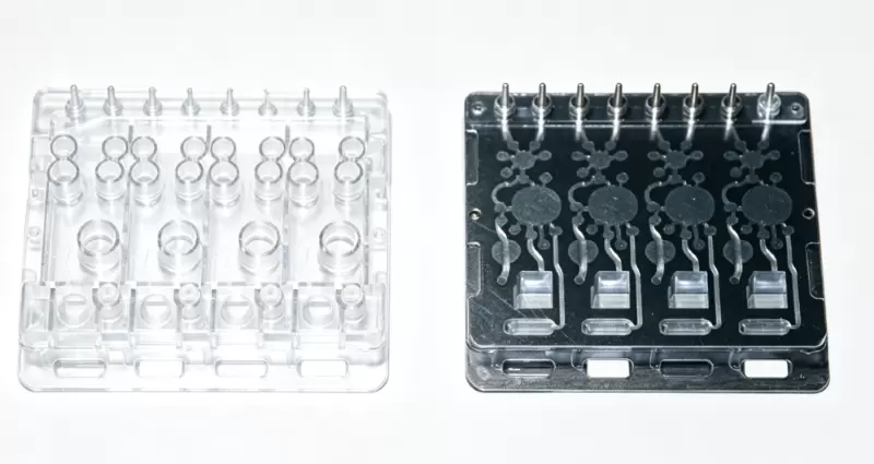
100–1000 pcs Hot embossing / CNC-machined thermoplastics Tens per unit
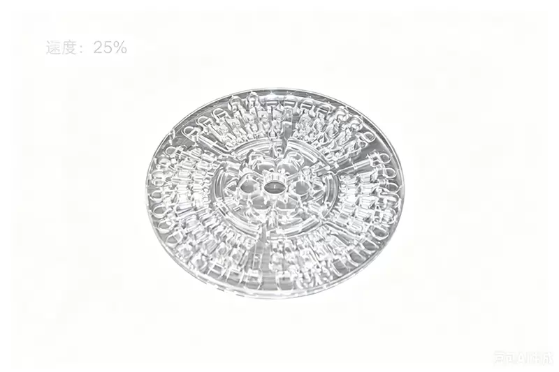
> 1000 pcs Injection molding (COC/COP) + steel tool Single-digit per unit, tooling capex in the low-to-mid hundreds of thousands
The break-even point for amortizing tooling generally falls between a few hundred and 1,000 pieces. Cut a steel tool below that and you are subsidizing samples with tooling money.
2. The application locks the material
Cell culture / organoids needing gas exchange → PDMS is irreplaceable (permeability is its core value, but the price is absorption of small-molecule drugs)
Organic solvents or high-temperature sterilization → glass / quartz
Integrated electrodes or sensors → silicon, or glass + ITO (electrodes must be defined before bonding; they cannot be modified afterwards)
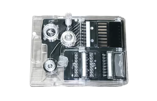
Disposable diagnostic cartridges → COC/COP, injection molded, UV transparent
Mass-spectrometry coupling → avoid PDMS; oligomer leaching contaminates the signal
3. The detection method constrains structure, not the other way round
Optical imaging requires a transparent substrate with consistent thickness. PDMS transmits light but its thickness uniformity is poor, so quantitative imaging drifts; for demanding work go straight to glass.
Timeline and risk expectations (empirical)
Design + simulation: 2–4 weeks
Photomask + master mold: 1–2 weeks (mask ~RMB 10k–20k per layer)
First PDMS prototype: within 1 week
Bonding process development + yield stabilization: 4–8 weeks — the step most likely to overrun
Injection mold + mold-flow analysis + trial shots: 8–14 weeks
From zero to production-ready: 3–6 months
The four most common pitfalls
Designing only the channels and not the world-to-chip interface. Everything ends up stuck on leakage and bubbles, and interface design effort is routinely underestimated by half.
Losing control of aspect ratio. PDMS channels above ~5:1 aspect ratio tend to roof-collapse; injection-molded features above ~10:1 do not fill completely. Feature width and depth must always be calculated together.
Holding thermal bonding right at the material's Tg. Channels deform on the spot. The process window normally needs to sit 20–30 °C below Tg.
Doing surface treatment once and then scaling up. Hydrophilicity decays over time, batch-to-batch results diverge, and the problem only surfaces at the customer.
Material selection reference
Material Minimum feature Volume cost Bonding Positioning
PDMS 20 µm High, hard to automate Plasma, easy Go-to for prototypes
COC / COP 20 µm Low, single-digit per unit Thermal / UV, medium Workhorse for volume cartridges
PMMA 50 µm Low Solvent-assisted, medium General-purpose lab parts
PC 100 µm Lowest Difficult Low-cost disposables
Glass / quartz 5 µm High Thermal / anodic, difficult High precision, chemical resistance
Silicon < 1 µm Very high Anodic / eutectic, difficult Electrode and sensor integration
Notes from the comparison cards:
PDMS — cast from a lithography master, sample in a week. Gas-permeable, which favors cell culture, but it absorbs small-molecule drugs.
COC / COP — injection molded, UV transparent, extremely low water uptake; the industry-standard material for diagnostic cartridges.
PMMA — works with both CNC and hot embossing, cheap to prototype; solvent and temperature resistance are only average.
PC — lowest unit cost, suited to coarse-channel consumables; poor solvent resistance and a very narrow bonding window.
Glass / quartz — resists aggressive solvents and high temperatures, best optical performance, good for imaging and MS coupling, but high unit price.
Silicon — sub-micron precision, direct electrode and sensor integration, but requires a MEMS line and is not transparent.
Bonding route by material
Material system Bonding method Process window Trade-off
PDMS Plasma activation bonding Room temperature, 30–60 s Moderate strength; must be mated immediately
Thermoplastics (COC / PC) Thermal bonding or UV adhesive 80–140 °C, 0.2–1 MPa High strength; channels prone to deformation
Glass / silicon Anodic bonding 400 °C + 400–1000 V Very high strength; requires a conductive layer
Customization requirement checklist
Fill this in before drawing the first design revision. Nine out of ten customization projects that fail do not fail because the process was infeasible — they fail because the requirements were never stated clearly. The "annual volume" line in particular determines whether you go PDMS or cut a steel tool.
Application and metrics
Application: culture / droplets / detection / synthesis
Sample type and volume per run
Flow rate range and maximum pressure
Detection modality: optical / electrical / mass spectrometry
Number of parallel channels and throughput requirement
Structure and material
Minimum feature size and aspect ratio
Substrate: PDMS / COC / PMMA / glass / silicon
Number of layers and bonding method
Interface: punched holes / Luer / sealed cartridge
Surface treatment and coating requirements
Delivery and compliance
Demand: prototype quantity / annual volume
Sterilization method and single-use vs. reusable
Biocompatibility level, ISO 10993
Quality system, e.g. ISO 13485
Delivery documentation: drawings / COA / yield report
Eight-stage workflow
Stage Focus Key output
1. Requirements definition Application, metrics, compliance Requirement spec / PRD
2. Design and simulation Channel network, CFD, Re / shear / residence time Verified layout, process window
3. Material selection Material dictates process Substrate and process route
4. Mold and master fabrication Photolithography, injection tooling SU-8 master or steel tool
5. Bonding and packaging The yield watershed Leak-tight, high-yield device
6. Surface engineering Hydrophilicity / hydrophobicity, antifouling, ECM coating Stable surface, batch-consistent
7. Verification and QC Leakage, metrology, biocompatibility Test data, COA, yield report
8. Scale-up Hardened tooling, yield ramp Production-ready supply

 English